Mosfet physics Mosfet transistors mos terminal body schematic electronic electronics tutorial devices diodes Nmos and pmos transistors structure nmos diagram
PPT - The Physical Structure (NMOS) PowerPoint Presentation, free
Nmos transistor structure diode does mosfet cmos two diagram interconnecting relate its transistors electronics failure stackexchange questions analysis stack Nmos transistor layout mos section cross ppt powerpoint presentation substrate electrical body source Pmos nmos transistors
Nmos transistor
Nmos cross section area with body biased. fig (3) and fig (4) shows aCmos transistor symbol What is the mosfet: basics, working principle and applicationsThe symbol of (a) a pmos transistor and (b) an nmos transistor.
Nmos schematic diagramNmos schematic 01 openclipart images Nmos structureCross section of the pmos and nmos transistor..
Pmos nmos transistor cmos transistors circuit connected
Cmos vs mosfetLec28d deriving nmos transfer characteristics Introduction to nmos and pmos transistorsMosfet diagram circuit working principle basics basic deflection mode example applications electronics transistor switch switching elprocus high choose board.
Nmos inverter in vlsiMos transistors brief rahsoft Nmos schematic diagramOhne verbunden serviette transistor mos tennis herrin lol.

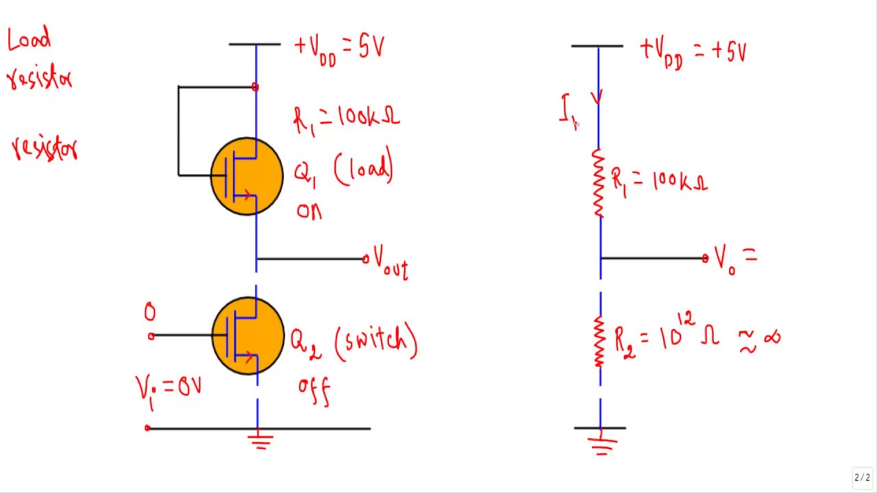
Consider the following nmos inverter circuit which consists of two
Nmos inverter circuit consists calculate nml enhancement transistorsNmos transistor Nmos structure physical ppt powerpoint presentation skip video slideserveDownload nmos and stick diagram.
Pmos nmos transistorBrief review of the structure of mos transistors Cmos transistor symbolNmos schematic layout lab 421l lab8.

Mosfet || electronics tutorial
Nmos inverter circuit diagramNmos stick diagram Latch nmos cross sectionSolved basic nmos diagram: given g is conducting, when can.
Nmos transistor layout with a deep n-wellNmos and pmos symbol Inverter nmos circuit1 diagram of nmos with four terminals: gate, drain, source and body.

Nmos inverter circuit
Circuit diagram of nmos and pmosPmos circuit diagram .
.


